Logo

Home | Audio | DIY | Guitar | iPods | Music | Brain/Problem Solving | Links| Site Map

This work is licensed under a Creative Commons License.
Through-Hole Soldering General Requirements

NASA

printed wiring board
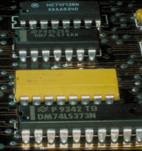
Discrete components are the backbone of the electronics world, consisting of individually packaged, leaded devices, highly integrated circuits (IC), interconnects, terminators, switches, etc.

While discretes are rapidly being displaced by the smaller-form surface mount technology (SMT) package, the discrete component is still widely in use, especially in extreme environmental applications where the SMT device will not perform reliability and/or is unavailable.

components on board
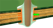
populated plated through hole with 100 percent solder fill

GENERAL REQUIREMENTS

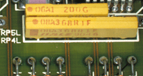
Components are installed per engineering documentation and are parallel to, and in contact with, the board surface. Component and board markings are clear and legible. Component leads exhibit proper bend radii and stress relief. Solder fillets are smooth and shiny with concave profiles.

PREFERRED

100% SOLDER FILL (PTH)
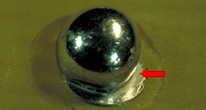
Populated plated through holes (PTH) should exhibit a vertical solder fill of 100%, with a fully formed fillet on the solder side, and evidence of 100% wetting on the component side lead, barrel and pad.


component with side fillet
solder side fillets

PREFERRED

PWB COMPONENT SIDE FILLET (PTH)
The solder joint surface is smooth, nonporous and undisturbed, with a finish varying from satin to bright. The fillet completely wets all elements to the periphery of the connection and is concave.


PREFERRED

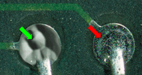
SOLDER SIDE FILLETS (PTH/NPTH)
The solder joint surfaces are smooth, nonporous and undisturbed, with a finish varying from satin to bright. The fillet completely wets all elements of the connection and is concave.


heat producing part
high mass components

PREFERRED

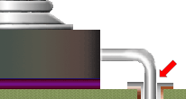
HEAT PRODUCING PARTS
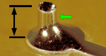
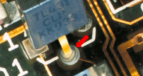
Parts which dissipate heat in quantities of 1 Watt or greater, or in quantities sufficient to damage the laminate shall be mounted with sufficient standoff [ > 1.5mm (0.060 in.) ] and shall be mechanically restrained.

PREFERRED

HIGH-MASS COMPONENTS
Components weighing in excess of 7 g (0.25 oz.) total, or 3.5 gm (0.12 oz.) per lead, shall be mechanically secured to the mounting surface by at least 4 evenly spaced bonds, when no other mechancial support is used.

minimum wire insulation gap
maximum wire insulation gap

PREFERRED

WIRE/LEAD INSULATION GAP
(MINIMUM)

The insulation shall not be imbedded in the solder joint. The contour of the conductor shall not be obscured at the termination end of the insulation.


PREFERRED

WIRE/LEAD INSULATION GAP
(MAXIMUM)

The termination exhibits a gap of less than two (2) insulated wire diameters (<2d) between the end of the insulation and the first point of contact of the conductor to the termination/pad.


adhesive holding component in postion on board
adhesive in the solder joint

ACCEPTABLE

ADHESIVES
Adhesives may be used to temporarily hold discrete components in position during wave or reflow soldering. Adhesives shall not interfere with soldering, and residues shall be removed following soldering operations.

UNACCEPTABLE

ADHESIVE INCLUSION
Adhesive material in the solder joint shall be cause for rejection.


clinched lead termination
improperly clinched lead

ACCEPTABLE

CLINCHED LEAD TERMINATION
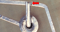
Conductor/lead ends may be clinched, with the clinched length at least 1/2 the largest solder pad dimension, bent in the direction of the longest pad dimension. Clinched leads shall not violate minimum electrical spacing requirements.


UNACCEPTABLE

IMPROPERLY CLINCHED LEAD
Component leads shall not be clinched toward an electrically uncommon conductor.


conductive case parts
solder dewetting

ACCEPTABLE

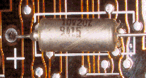
CONDUCTIVE CASE PARTS
Parts having conductive cases, which are mounted over printed conductors or which are in close proximity to other conductive materials shall be separated by insulation of suitable thickness, or shall have an insulating jacket/sleeve.


ACCEPTABLE

DEWETTING
Slight solder dewetting around the periphery of the component side termination pad shall not be cause for rejection, provided the termination exhibits flow-through and bonding of the lead/conductor to the termination pad.


exposed base metal
exposed base metal

ACCEPTABLE

EXPOSED BASE METAL
Exposed ends of leads on straight-through termination shall not be cause for rejection if the PWA is to be conformally coated.


UNACCEPTABLE

EXPOSED BASE METAL
Defects or damage (cuts, nicks, gouges, scrapes, etc.) that result in exposed base metal (except for the vertical edges of circuit traces, lands and pads) shall be rejectable.


exposed base metal
filler wire

ACCEPTABLE

EXPOSED BASE METAL
(SPECIAL EXCEPTION)

Exposed base metal on the vertical edge of printed wiring conductors, lands and pads is acceptable.


ACCEPTABLE

FILLER WIRE USE
Interfacial connections in double-sided PWBs require the use of filler wire if the PWB coupon is not evaluated by construction analysis.


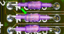
glass encased parts
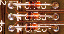
unsleeved glass encased parts

ACCEPTABLE

GLASS ENCASED PARTS
Glass encased parts shall be covered with transparent/translucent resilient sleeving (or other approved material) when epoxy is used for staking, conformal coating, encapsulating or where damage from other sources is likely.


UNACCEPTABLE

UNSLEEVED GLASS ENCASED PARTS
Glass encased parts shall be covered with transparent/translucent resilient sleeving (or other approved material) when epoxy is used for staking, conformal coating, encapsulating or where damage from other sources is likely.


lead protrusion
insufficient lead protrusion

ACCEPTABLE

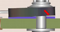
LEAD PROTRUSION LENGTH
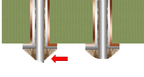
Leads terminated straight through the PWB shall extend 0.5 mm (0.020 in.) to 2.29 mm (0.0900 in.) beyond the pad surface. Leads may be bend up to 30° from the vertical plane to retain the part during soldering.


UNACCEPTABLE

INSUFFIENCT LEAD PROTRUSION
Leads terminated straingt through the PWB shall extend a minium of 0.5 mm (0.020 in.) beyond the pad surface.


interfacial connections on multi layer printed wiring board
solder filler interfacial connections

ACCEPTABLE

INTERFACIAL CONNECTIONS/VIAS
(MULTILAYER PWBs)

Interfacial connections (vias) in multilayer PWBs do not require the use of filler wire, and shall not be solder filled.


ACCEPTABLE

SOLDER-FILLED INTERFACIAL
CONNECTIONS (PTH/VIAS)

No dedicated effort shall be expended to remove solder from unpopluated plated through holes (PTH) and/or vias.


measling
measling

ACCEPTABLE

MEASLING
Whitish, discrete spots or crosses below the laminate surface - usually induced by thermal shock/stress. Measling that bridges uncommon conductors is unacceptable.


UNACCEPTABLE

MEASLING
Measling that bridges uncommon conductors is unacceptable.


uneven flow of solder fillet

ACCEPTABLE

NON-UNIFORM/UNEVEN FLOW
(DEMARCATION LINES/FILLET SWIRLS)

A solder fillet exhibiting a nonuniform/ uneven profile, demarcation lines or swirls is acceptable, provided the fillet is shiny and there is evidence of complete wetting with smooth fillets at the swirls.

UNACCEPTABLE

UNEVEN FLOW/REFLOW
A solder fillet exhibiting nonuniform/ uneven flow lines/swirls with hard demarcation lines (no fillet at swirl interfaces), and a dull finish are typically caused by an inadequate/uneven application of heat during the fillet formation.


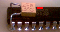
part markings
component with identification marks hidden

ACCEPTABLE

PART MARKINGS
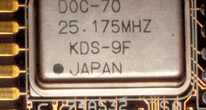
Parts shall be mounted in such a manner that, at a minimum, the markings are visible in the following order of precedence: polarity, traceability/lot code (if applicable), part value, part number/type.


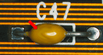
UNACCEPTABLE

IDENTIFICATION MARKS MISSING
The component (capacitor C47) has been mounted with the identification marks on the underside of the component body (against the circuit board), preventing visual confirmation that the correct value part is installed.


pits in the solder
transparent shrink tubing

ACCEPTABLE

PITS
A solder pit is acceptable, provided the bottom of the cavity can be seen from all angles of vision.

ACCEPTABLE

SHRINK TUBING
(TRANSLUCENT/TRANSPARENT)

Shrink tubing installed over components and/or soldered terminations shall be transparent (or translucent) to allow visual inspection.


smooth tool impression marks
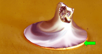
solder fillet recess

ACCEPTABLE

SMOOTH TOOL IMPRESSION MARKS
Smooth tool impression marks (slight cuts, nicks, scratch or scrapes) on the conductor surface, which do not expose base metal or reduce cross-sectional area are acceptable.


ACCEPTABLE

SOLDER FILLET RECESS/SHRINKBACK
A slight recessing or shrinkback of the solder into the PTH below the solder pad is acceptable, providing the lead and pad exhibit wetting and the shrinkback is slight.


solder in stress relief bend

ACCEPTABLE

SOLDER IN STRESS RELIEF BEND
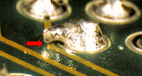
Solder which extends into the stress relief bend of any leaded part shall not be cause for rejection if the topside bend radius is discernable, and if the solder does not extend within one (1) lead diameter of the part or end seal.


UNACCEPTABLE

SOLDER IN STRESS RELIEF BEND
Solder extends into the stress relief bend and contacts the part body end seal. The topside of the lead is not discernable.


tempered leads
bent tempered leads

ACCEPTABLE

TEMPERED LEADS
Tempered/hardened leads (sometimes referred to as pins) shall not be bent or formed for mounting purposes since body seals and connections internal to the part may be damaged.


UNACCEPTABLE

BENT TEMPERED LEADS
Tempered/hardened leads (sometimes referred to as pins) shall not be bent or formed.


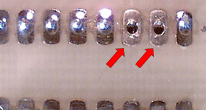
blowhole in solder
bridging of conductors

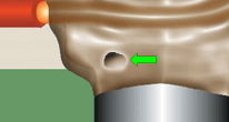
UNACCEPTABLE

BLOWHOLE
Blowholes are typically caused by trapped gases or flux during the formation of the solder fillet, and are unacceptable.


UNACCEPTABLE

BRIDGING
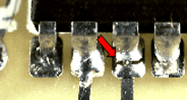
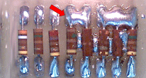
Bridging is an indicator of poor process controls (i.e.: excess solder, smeared paste, improper placement, incorrect heat).


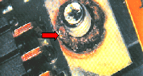
component with charring
component with nicks

UNACCEPTABLE

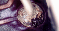
CHARRING
Charring of components and/or laminate is an indicator or poor process control (i.e.: excessive heat).


UNACCEPTABLE

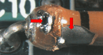
CHIP-OUTS (NICKS)
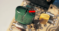
The use of parts with chips in the component body, termination area or meniscus, is prohibited.


cold solder joint
contamination of lamination

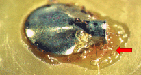
UNACCEPTABLE

COLD SOLDER JOINT
A cold solder joint is an indicator of incorrect process control (i.e.: inadequate heat).


UNACCEPTABLE

CONTAMINATION
Contamination is a reliability concern.


coplanarity of leaded parts
component with cracks

UNACCEPTABLE

COPLANARITY
Improper coplanarity of leaded parts will result in bridging, shorts, opens and/or misalignment. Part leads shall be reworked (if allowed) prior to installation.


UNACCEPTABLE

CRACKS (COMPONENT)
Cracks (especially in ceramic components) are an indicator of poor process control (i.e.: improper preheat, thermal/ mechancical shock, etc.).


cracks in the laminate
cracks in the solder fillet

UNACCEPTABLE

CRACKS (LAMINATE)
Cracks in the laminate are cause for rejection.


UNACCEPTABLE

CRACKS (SOLDER FILLET)
Cracks or fractures in the solder fillet are an indication of mechanical/thermal shock, or temperature coefficient mismatch.


damaged part seal
dewetting of solder

UNACCEPTABLE

DAMAGED PART SEAL
Parts with damaged seals shall not be used.


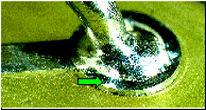
UNACCEPTABLE

DEWETTING
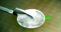
Dewetting is caused when molten solder coats a surface and then recedes, leaving irregulary-shaped solder deposits separated by areas covered by a thin solder film.


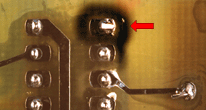
discolored laminate
discolored laminate

UNACCEPTABLE

DISCOLORED LAMINATE (BURNS)
Burns that physically damage the laminate surface of the assembly are not allowed. Slight discoloration is allowable.


UNACCEPTABLE

DISCOLORED LAMINATE
(OVERHEATING)

A browning/darkening of the laminate because of excess heat; an indicator of improper process control/ thermal design.


disturbed solder
excess solder

UNACCEPTABLE

DISTURBED SOLDER
A disturbed solder joint is characterized by the appearance that there was motion between the metals being joined while the molten solder was solidifying.


UNACCEPTABLE

EXCESS SOLDER
The solder fillet shall exhibit a positive wetting angle and shall not contact the component body.


solder flooding
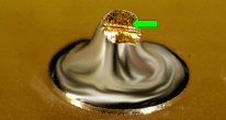
excessive lead protrusion

UNACCEPTABLE

EXCESS SOLDER/SOLDER FLOODING
Excess solder/Solder flooding is an indicator of improper/incorrect process controls, and is typically seen in wave soldering.


UNACCEPTABLE

EXCESSIVE LEAD PROTRUSION
Leads terminated straight through the PWB shall extend a maximum of 2.29 mm (0.090 in.) beyond the pad surface. Leads may not violate minimum electrical spacing requirements.


exposed circuit elements
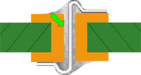
eyelet

UNACCEPTABLE

EXPOSED DIE/CIRCUIT ELEMENTS
The unprotected exposure of die or circuit elements is not allowed unless specified in the engineering documentation.


UNACCEPTABLE

EYELETS
Eyelets shall not be used for interfacial terminations.


flux residue
flux splatter

UNACCEPTABLE

FLUX RESIDUE
Flux residue indicates improper/ incomplete cleaning.


UNACCEPTABLE

FLUX SPLATTER
Flux splatter is an indication of an improper process parameter (heat/moisture).


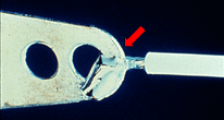
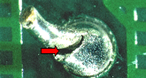
fractured solder
gold intermetallic

UNACCEPTABLE

FRACTURED SOLDER
A fractured solder joint is an indication that the joint has been subjected to extreme mechanical shock. A crack in an "as-received" assembly is unusual and cause for concern.


UNACCEPTABLE

GOLD INTERMETALLIC
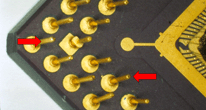
Gold intermetallic is characterized by evidence of golden colored streaks in the solder fillets of gold plated leads that have not been properly tinned. Gold intermetallic can severly embrittle a solder joint.


gold plating
hole obstruction

UNACCEPTABLE

GOLD PLATING
Gold plated surfaces that will become part of the finished solder connection shall be tinned prior to soldering to remove the gold plating.


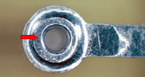
UNACCEPTABLE

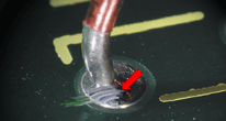
HOLE OBSTRUCTION
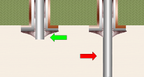
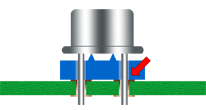
The mounting pad has been installed upside down. Parts shall not be mounted such that they obstruct solder flow to the component-side termination area (pad) or prevent cleaning and inspection.


lead bending
lead cutting

UNACCEPTABLE

IMPROPER LEAD BENDING
The minimum distance from the part body/seal to the start of the bend shall be 2 lead diameters for round leads and 0.5 mm (0.020) for ribbon leads. The bend radius shall not be less than one lead diameter (1 d) or ribbon thickness (1 t).


UNACCEPTABLE

IMPROPER LEAD CUTTING
Leads shall be cut per engineering documentation and by methods, which do not impart stress to the lead seal or internal terminations.


improper lead length
improper orientation

UNACCEPTABLE

IMPROPER LEAD LENGTH
The clinched lead extends beyond the pad edge in excess of allowed limits and is bent over an uncommon electrical conductor.


UNACCEPTABLE

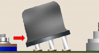
IMPROPER ORIENTATION
Parts shall be mounted parallel to the laminate surface, right side up and aligned to the lands within design and engineering specifications.


improper tinning
insufficient solder

UNACCEPTABLE

IMPROPER TINNING
Tinned surfaces, which are to become part of the solder termination, shall exhibit 100% coverage.


UNACCEPTABLE

INSUFFICIENT SOLDER
Insufficient solder is an indicator or improper process control, and may result in reduced reliability.


insufficient stress relief
meniscus contact

UNACCEPTABLE

INSUFFICIENT STRESS RELIEF/LEAD BEND
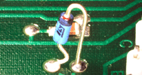
Lead is improperly bent, placing strain on the weld bead. Conductors and part leads shall have sufficient stress relief to prevent damage to the solder termination and/or part.


UNACCEPTABLE

MENISCUS CONTACT
Parts exhibiting contact with, or embedment of the meniscus and the solder joint, shall be rejected.


component body with nicks
nonwetting of solder

UNACCEPTABLE

NICKS
The use of parts with nicks in the component body or termination area is prohibited.


UNACCEPTABLE

NONWETTING
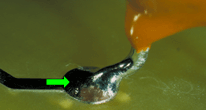
Nonwetting results in the solder forming a ball or beading on the termination surface. The fillet is convex; no feathered edge is apparent.


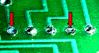
no flow of solder
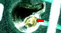
no solder in hole

UNACCEPTABLE

NO FLOW/REFLOW
The lack of flow/reflow of solder is an indicator of poor process control or layout design (i.e.: inadequate heat, shadowing).


UNACCEPTABLE

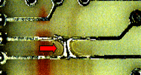
NO SOLDER
The lack of solder is an indicator of poor process control.


obscured solder teminations
voids in solder

UNACCEPTABLE

OBSCURED SOLDER TERMINATIONS
The placement of a part, which obscures the inspectability of another part's terminations, is unacceptable, unless interim inspection is performed (part depicted is mounted over previously installed surface mount components).


UNACCEPTABLE

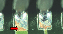
OPENS/VOIDS
Cavities (opens/voids) reduce the circumferential wetting of lead and barrel, land coverage and vertical solder fill below minimum acceptable requirements.


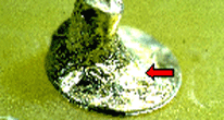
overheated solder
part body contact

UNACCEPTABLE

OVERHEATED SOLDER
Overheated solder has a dull, gray, frosty and/or crystallized appearance and is the result of excessive exposure to heat.


UNACCEPTABLE

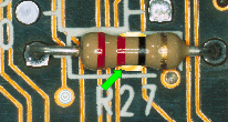
PART BODY CONTACT
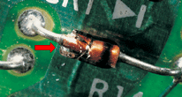
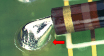
Part bodies shall not be in contact with soldered terminations. The spacing between components is below recommended values, resulting in contact between the resistor body and the lead, which may eventually result in a short circuit.


part lead used as terminal
part misalignment

UNACCEPTABLE

PART LEADS USED AS TERMINALS
Part leads shall not be used as terminals, unless the part lead is designed to function as a terminal.


UNACCEPTABLE

PART MISALIGNMENT
Part misalignment is an indicator of improper process control.


piggybacked part
pinhole in solder

UNACCEPTABLE

PIGGYBACKED PARTS
The piggybacking of parts not designed specifically for that configuration is prohibited.


UNACCEPTABLE

PINHOLE
Pinholes are typically small holes in the solder surface, leading to a void of indeterminate size within the solder termination.


poor wetting of solder
popcorning between component parts

UNACCEPTABLE

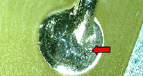
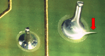
POOR WETTING
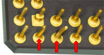
Poor wetting is an indicator of poor solderability, improper flux or contamination.


UNACCEPTABLE

POPCORNING
Popcorning is caused by the release of entrapped moisture during the soldering process.


porous solder
rosin solder joint

UNACCEPTABLE

POROUS SOLDER
Porous solder exhibits an uneven surface and a spongy appearance that may contain a concentration of small pinholes and voids.


UNACCEPTABLE

ROSIN SOLDER JOINT
A rosin solder joint is similar in appearance to a cold solder joint, but exhibits evidence of entrapped flux in the fillet and at the surfaces to be joined.


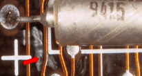
scratches on solder fillet
solder ball

UNACCEPTABLE

SCRATCHES (SOLDER FILLET)
Scratches in the solder are prohibited.


UNACCEPTABLE

SOLDER BALLS
Solder balls are considered a contaminant and are an inedciation of improper process control (inadequate preheat) and/or the use of outdated solder/flux.


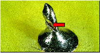
solder peaks
solder skips

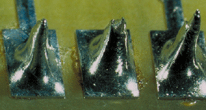
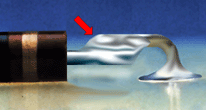
UNACCEPTABLE

SOLDER PEAKS, ICICLES, SHARP EDGES
Solder peaks, icicles and/or sharp edges are an indicator of an improper process parameter and are a reliability and short-circuit concern.


UNACCEPTABLE

SOLDER SKIPS
Solder skip is the random non-formation of solder fillets, and is an indicator of poor process control. Solder skip may be caused by insufficient solder, contamination, non-solderability (oxide), improper flux, solder thieving, etc.


solder slivers
solder splatter

UNACCEPTABLE

SOLDER SLIVERS
Solder slivers are an indication of improper process control.


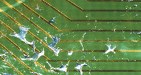
UNACCEPTABLE

SOLDER SPLATTER
Solder splatter is typically caused by moisture contamination and is an indicator of poor process control.


solder webbing
spliced conductor

UNACCEPTABLE

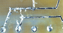
SOLDER WEBBING
Webbing is an indication of improper process control.

UNACCEPTABLE

SPLICED CONDUCTORS/LEADS
Splices shall not be used to repair broken or damaged conductors or part leads.


voids in solder
whisker on the lead

UNACCEPTABLE

VOIDS
Voids are an indication of improper process control, and are typically caused by insufficient solder, solder wicking/thieving or contamination.


UNACCEPTABLE

WHISKER
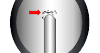
A whisker is a slender needle-shaped metallic growth between a conductor and a land. Typically the result of mechanical stresses in high tin compounds, it is a reliability concern.


Home | Audio | DIY | Guitar | iPods | Music | Links | Site Map | Contact

Top

Creative Commons License